EMST - Ensinger Microsystems Technology
The development of products and technologies in fields such as mobility, medical, electronics and energy would be inconceivable without microsystems or microelectromechanical systems (MEMS). The current framework conditions impose high demands on microsystem manufacturers, with complex and cost-intensive production processes, sophisticated machinery, and labor-intensive back-end processes limiting possibilities. Progress in the microsystems sector is further hindered by issues such as raw material scarcity and technological limitations.
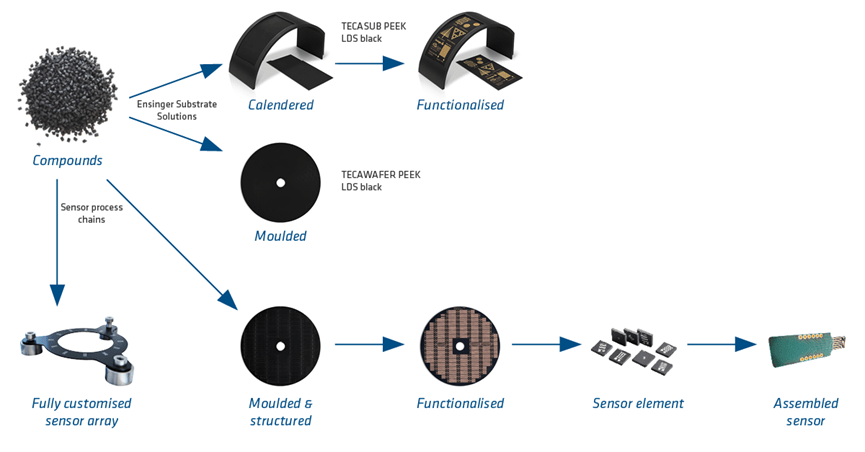
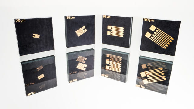
Ensinger Microsystems Technology (EMST) offers a completely new approach. As the world's first manufacturer, we seamlessly combine MEMS technology with the advantageous properties of high-performance plastics. EMST's revolutionary approach transforms microsystems and MEMS manufacturing, combining functionalisation and seamless integration to provide individualised solutions for functions, shapes, volumes, and sizes.
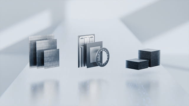
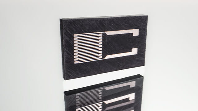
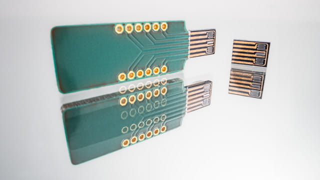
With EMST, we offer solutions to many existing challenges in MEMS technology. New possibilities for functionalisation, integration and customisation enable revolutionary approaches across industries. With innovative contact options that combine both sides, our materials are easy to process, paving the way for shorter, simpler and more cost-effective process chains, even for custom solutions. Our solutions based on high-performance plastics easily overcome challenges such as heat resistance, outgassing and chemical resistance.
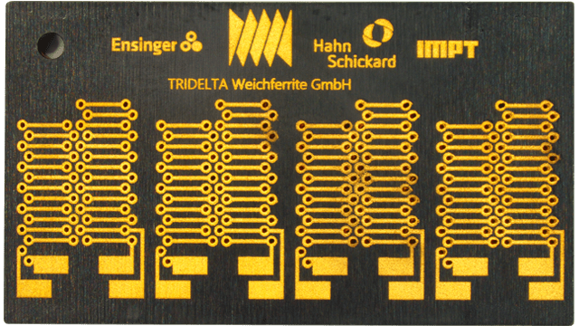
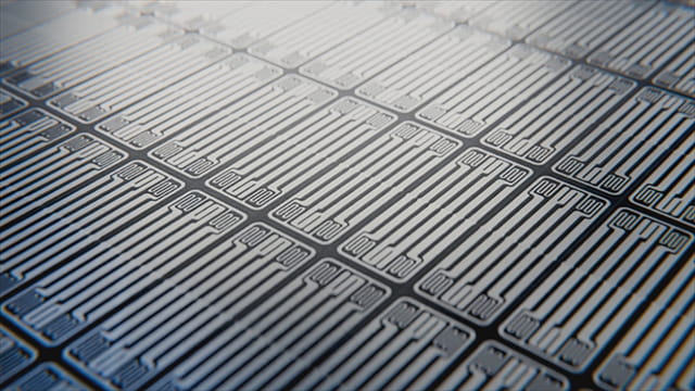
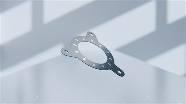
Ensinger Microsystems Technologies approach allows complete microsystems manufacturing outside cleanroom environments. Utilising high-performance PEEK (TECACOMP PEEK LDS) as a substrate simplifies conductor track application, eliminating cleanroom requirements and reducing the overall steps to achieve precision. With our new microsystems technology, we reduce back-end processes significantly.
Choose sustainability and a secure supply chain with our recyclable thermoplastics. With our own development and production facilities in Germany, we are well equipped to develop customised solutions that add value to your application.
Ready to take your application to the next level? Ensinger Microsystems Technology makes it possible. It's not just any material, it's PEEK.