PEEK-based substrates like TECAWAFER and TECASUB are an innovative alternative to traditional substrate materials such as silicon, ceramics, and glass, unlocking new possibilities in microsystems technology. Our plastic substrates offer beneficial properties that no other material offers, including high thermal and chemical resistance, enhanced design freedom and simplified processes, as well as industry-specific solutions.
Unlike conventional materials, which often present limiting properties and depend on global supply chains prone to delays and losses, TECAWAFER and TECASUB provide flexible design options while reducing both capital and production costs. Material availability and short supply chains minimise reliance on global networks. Replace traditional materials with innovative plastics to benefit from increased flexibility and optimised efficiency across various applications.
TECAWAFER and TECASUB bridge the gap to conventional materials, delivering cutting-edge solutions for your needs.


When choosing between TECASUB and TECAWAFER, it is essential to consider the specific requirements of your application. Learn more about Ensinger Substrate Solutions below or contact us for tailored advice to help you determine the right solution for your application.

TECAWAFER offers superior precision and excellent surface quality, making it the better choice for applications where high surface characteristics are critical.

TECASUB is ideal for cost-efficient and flexible production without size limitations, making it particularly suited for various microsystem sizes.
TECAWAFER: Pushing the Boundaries of Substrate Technology with PEEK
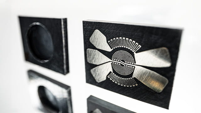
TECAWAFER, our 4-inch wafer made from TECACOMP PEEK LDS, is offering a superior alternative to silicon, ceramic, and glass wafers and is compatible with existing process chains. Its LDS capability simplifies assembly and connection technology and offers benefitial properties such as low thermal conductivity, high elasticity, and resistance to aggressive environments. TECAWAFER optimises frequency behaviour, surpasses silicon in dielectric strength, and supports flexible machining methods like laser cutting. Made in Germany, it combines sustainability with innovation, featuring short supply chains and a low carbon footprint.
TECAWAFER has a particularly good surface roughness, achieved without any post-treatment. The standard surface roughness of TECAWAFER is at 20-30 nanometres Ra. For special applications, we can also realise roughnesses below 10 nanometres Ra. This allows us to achieve optimum surface qualities, suitable even for highly demanding applications such as those used in optics.
TECAWAFER can be further processed by standard lithography, PVD or PECVD processes and structured by LDS processes. PVD coatings, CVD coatings and various other processes such as ALD or PECVD can applied for thin film systems. A combination of conventional lithography, PVD coating and now LDS structuring, known from 3D-MID technology, offers completely new possibilities for the assembly and interconnection of thin film based microsystems.
By using the high performance polymer PEEK, TECAWAFER is chemically and temperature resistant, and electrically insulating. PEEK is also not thermally conductive to the same extent as silicon, glass or ceramics. As a result, TECAWAFER offers additional material-specific advantages compared to the conventional wafers available on the market.
Unlike conventional substrates, thermoplastic PEEK can be recycled. TECAWAFER is also much less energy intensive to produce than, for example, silicon, glass or ceramics. This also supports the sustainability goals of many applications and industries.


Our substrates combine low thermal conductivity, high elasticity, and exceptional acid resistance, making them ideal for demanding applications in sensor and electronics technology. Compared to conventional substrates, they offer additional advantages such as high dielectric strength and optimal frequency performance, surpassing silicon. Our TECAWAFER substrates also feature improved surface roughness and flatness compared to ceramic materials, ensuring a reliable solution for industrial processes and setting new benchmarks in microsystems technology. The added LDS capability opens up innovative approaches for interconnect technology (AVT), enhancing design possibilities and efficiency in advanced manufacturing processes.
Due to low thermal conductivity, our substrates are particularly suited for applications such as temperature sensors, flow sensors, and heating elements where minimal heat transfer is crucial.

Our substrates streamline production by minimising process steps, maximising design freedom, and reducing investment costs. They provide efficient adapter and interposer solutions, enabling easy realisation of VIAs and bridging the gap between ICs and PCBs with a simplified electrical infrastructure and straightforward interconnect technology (AVT).
These substrates offer extensive design freedom through laser cutting, simple mechanical processing such as milling and drilling, and options for welding or passivation with PEEK film substrates.
By eliminating the need for additional process steps such as insulation, grinding, and PVD coating, our solution enhances efficiency and reduces production complexity, resulting in lower equipment investment costs.
Support flexible and precise customisation through laser cutting, milling, drilling, and options for welding or passivation with PEEK film.

With our innovative substrate materials, we also offer tailor-made solutions for your requirements in microsystems technology and sensor technology.
In the area of conventional microsystems design and manufacturing, we offer additional services such as laser cutting, mechanical processing like milling and drilling, as well as passivation with PEEK film.
Additionally, we also offer a new approach for completely individual applications: Ensinger Microsystems Technology (EMST) offers solutions that can be functionalised, integrated and fully customised, with a wide range of options, including sensor size and form, wafer and batch sizes and specific functionalisation, integration and packaging options.
Contact our experts for more information on our services.