PCB testing equipment

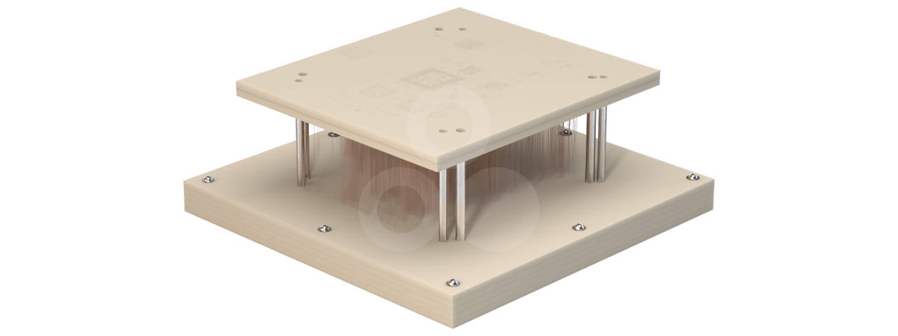
PCB Inspection Fixtures

Printed Circuit Boards (PCBs) serve as the platform for linking electrical components and connectors and are used in almost all electronic devices. During the fabrication and assembly process, PCBs must undergo thorough inspections to ensure that the product functions correctly. As PCBs have gotten more complex and advanced, so have the inspection techniques used to check for shorts, opens, or malfunctioning solder joints, and to ensure that performance values are within the required tolerance levels. 

PCB inspection fixture made from PPS, TECATRON natural
Functional testing with PCB inspection equipment includes the use of  PCB testing fixtures or testing jigs. The fixture’s top hat includes an array of nails pressed against the PCB, simulating the electrical environment of the final application. As the test points on the PCBs are minimal, the encountering array of test-probe points on the contact plate need to be highly dense. In recent years, finer pitch and smaller probe diameter requirements have become more commonplace, in some cases requiring up to 3000 probe points per square centimeter, with diameters down to 20 µm. Usually, multiple thin sheets are stacked for the contact plate, as the machining of micro-holes requires the plate to be as thin as possible, while a thick and rigid contact plate is preferred to avoid bending. In some cases, only the areas with holes have reduced thickness, while the areas without holes are kept thicker to maintain rigidity. The filigree design of the PCB inspection fixture creates the greatest challenge for the structural material that is to be used for the contact plates and fixture body. 

PPS plastic - a good choice but with challenges

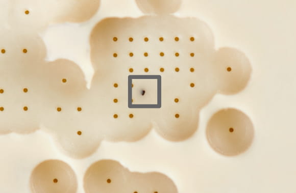
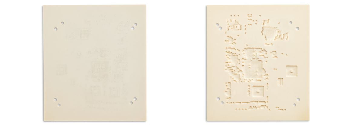
From a range of different semiconductor plastics, PPS is often chosen for this application due to the high requirements. This is because drilling micro-holes for inserting the wire probes requires a material with a balanced ratio of stiffness and ductility to ensure minimal burr formation and cracking.

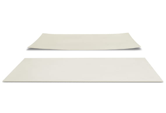
The material also needs to be dimensionally stable with minimum water absorption and thermal expansion levels to ensure the array of holes remains within tolerance. Besides the influence of the material itself, dimensional stability is also influenced by the molding technique, as residual stress can result in warpage while machining. Moreover, a material with higher wear resistance is preferred, as the wire probes abrade the inner wall of the contact plate while the fixture is pressed against the PCB.

However, not every PPS material is equally suitable, as the extrusion of PPS is characterised by a number of challenges. For this reason, in cooperation with leading manufacturers of components for PCB inspection equipment, we have developed Ensinger's TECATRON SX natural, a material made of polyphenylene sulfide (PPS), which has characteristics that make it particularly suitable for contact plates and and fixture body parts.

Making the perfect match in semiconductor plastics

PPS plates internal stress comparison
black speck on PPS material
Due to ever thinner sheet requirements and increasing needs for micro-holes, common issues such as deformation and warpage are due to residual stress found in the material. Moreover, optical issues like flow marks and black specks resulted in a reduced manufacturing process yield. Choosing TECATRON SX natural enabled higher production yield due to minimized residual stresses, allowing flatness even when thinning down large sheets at once. Furthermore, the molding process of TECATRON SX natural has been optimized to reduce optical issues, which also impacts the yield when producing PCB inspection fixture parts.
If you zoom and rotate here, you can take a closer look at the PCB inspectionfixture, made by Ensinger from TECATRON SX.