The market for sensor applications is a big one: large numbers of microsystems are used in the IT and telecommunications sector, the automotive and aerospace industries, and mechanical and plant engineering. These electronic components are based on ‘wafers’ – thin slices of material, usually silicon, onto which thin films are applied. The production and further processing of silicon wafers is very labour-intensive and costly. The Institute of Micro Production Technology, part of the Leibnitz University Hannover (IMPT), has investigated alternative production methods for sensor applications. A study showed that modified polyetheretherketone (PEEK) can replace high-cost substrates such as silicon. To make a function demonstrator (temperature and magnetic field sensor) using injection moulding with laser direct structuring (LDS), the material TECACOMP PEEK LDS black 1047045 – a high-performance compound from Ensinger – was used.
The production of an enclosed sensor which can be easily integrated into assembly processes for printed circuit boards comprises, with the LDS method, three production steps:
In the first step, the substrates are produced from laser-activatable plastic in an injection moulding process. This incorporates predefined sensor structures as well as vertical interconnect accesses (VIAs) for through-connections. The next step is the laser drilling of recesses and the activation of the LDS-compatible polymer by means of current-free, selective precipitation of metals. Subsequently an unstructured sensor layer is applied by means of cathode sputtering. The required structures are then exposed in a CMP process (chemical mechanical polishing).
Using injection moulding with laser direct structuring reduces the complexity in manufacturing and packaging processes. Unlike conventional silicon-based wafer production, the LDS mothod does not require a cleanroom environment or photolithography.
As well as reducing the number of process steps, the use of laser-activatable high-performance polymers instead of silicon as a substrate for wafer manufacture can also bring significant cost benefits for production. Stefan Bur, Application Segment Manager for MID/LDS at Ensinger, sees huge potential in this innovative application: “In the electronics sector, the polymer PEEK in particular is becoming increasingly important thanks to its special properties. The study by the IMPT has shown that our compound TECACOMP PEEK LDS, which is unique on the market, can be used as a wafer material. In initial applications, the sensor displayed around 75 percent of the performance capacity of a conventional, silicon-based sensor. The manufacturing costs showed potential savings of 90 percent.” Ensinger is confident that in the future, small and medium-sized companies will also be in a position to produce cost-effective wafers for microsystem technology using the LDS method. “For this reason we are investing in the development of these compounds. Our new product, TECACOMP PEEK LDS grey, is already optimised for applications that place particularly high demands on surfaces”, explains Stefan Bur.
TECACOMP PEEK LDS compounds may be of interest for sensors in electrical engineering, mechanical engineering and medical technology. Potential areas of application are position sensors (AMR and GMR sensors), eddy current sensors, temperature sensors for measurements in the laboratory or industrial processes (thin-film Pt sensors), or DC converters.
When it comes to manufacturing microsystems, the LDS makes particularly high demands of the polymer. For many years now, Ensinger has been developing thermoplastic compounds for laser direct structuring and is currently the only plastics specialist who can offer a PEEK certified for the LDS method by LPKF Laser & Electronics AG. TECACOMP PEEK LDS black 1047045 is optimised with mineral fillers. The material is extremely temperature-resistant (up to 260°C, long-term), has very good weld strength, good adhesive strength and shows high chemical resistance to solvents. Furthermore, TECACOMP PEEK LDS has a very low coefficient of linear thermal expansion - one which is closer to that of metals than that of many other plastics.
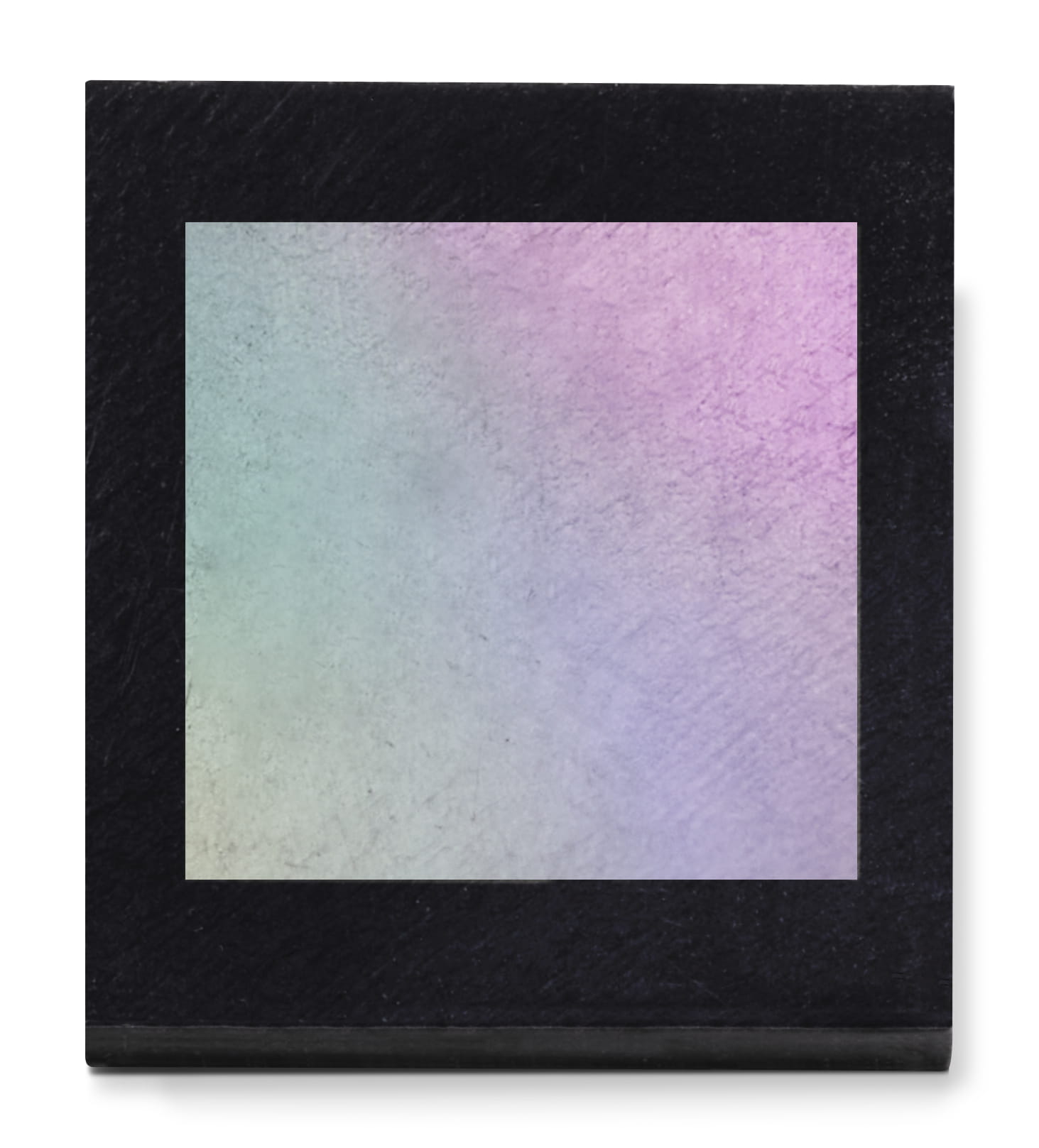
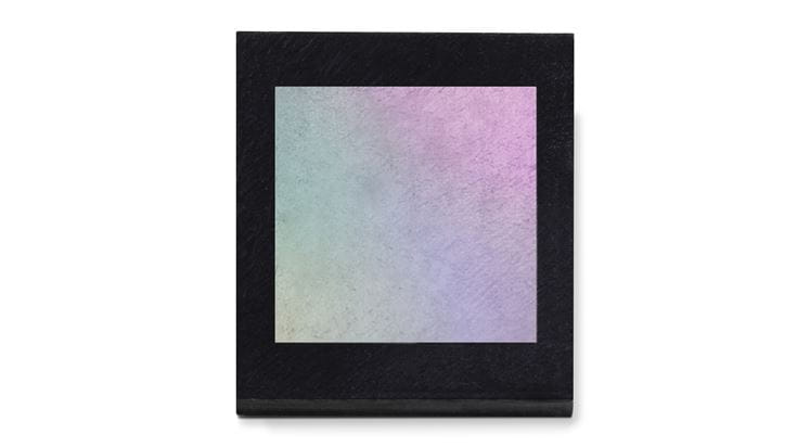 The illustration shows microstructures (Bragg grating) on a sensor. The compound TECACOMP PEEK LDS black 1047045 made by Ensinger is extremely temperature-resistant, has very good weld line strength, good adhesive strength and shows very high chemical resistance to solvents. Furthermore, the material has a very low coefficient of linear thermal expansion (Photo: Ensinger / IMPT)
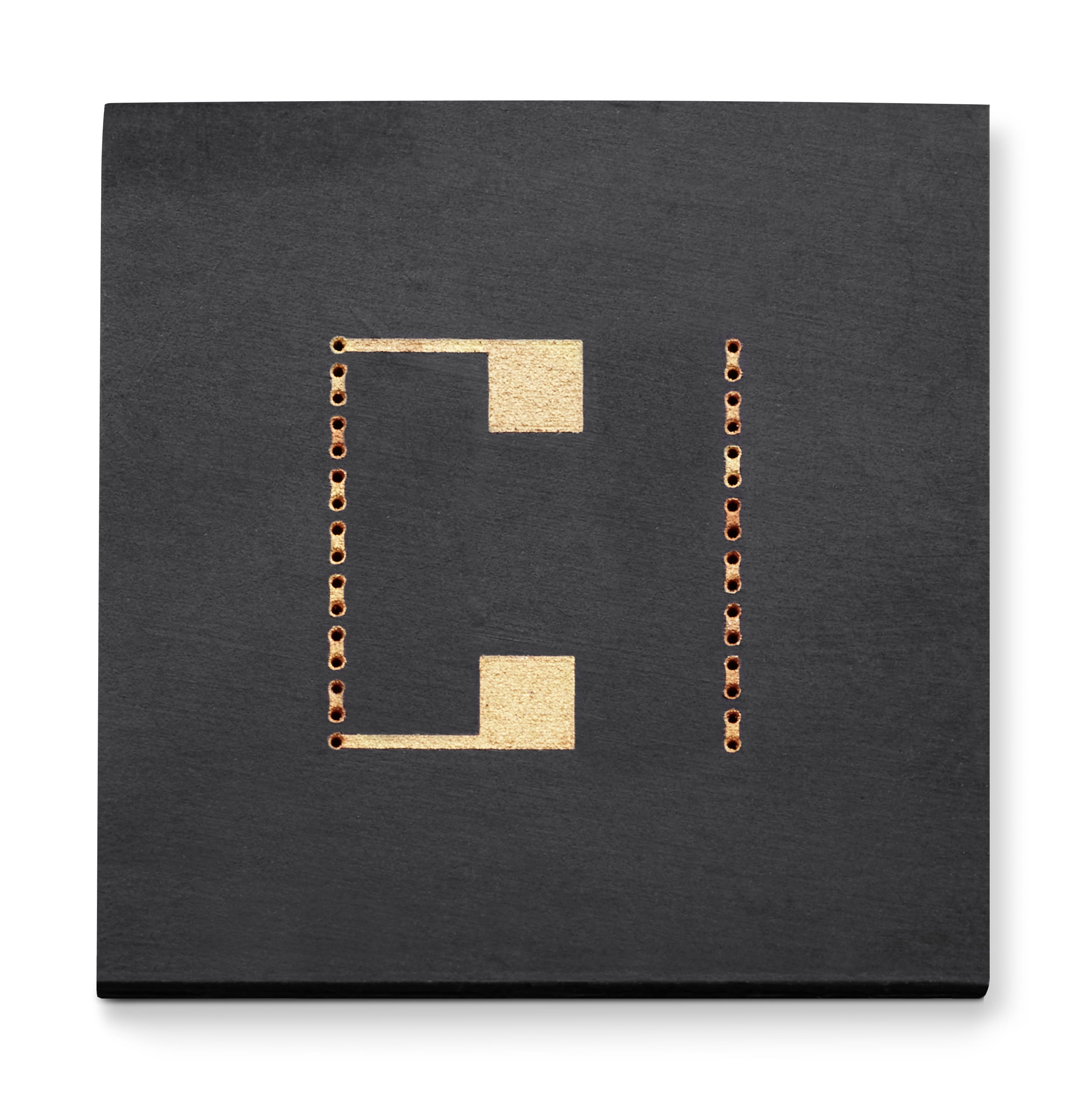
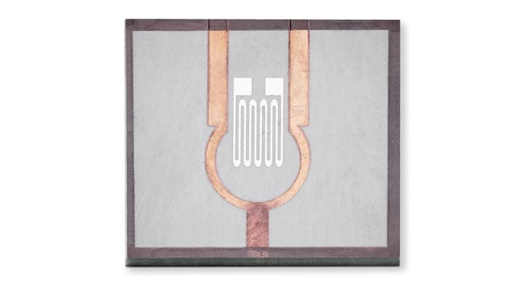 Eddy current sensor. For its manufacture by means of the LDS method, the compound TECACOMP PEEK LDS grey is used. This new product variant from plastics processor Ensinger fulfils particularly high surface requirements (Photo: Ensinger / IMPT)
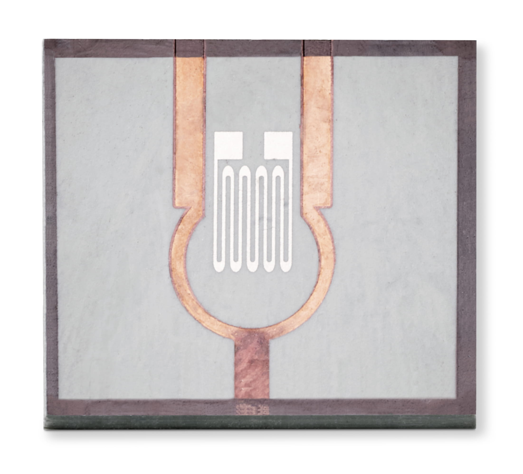
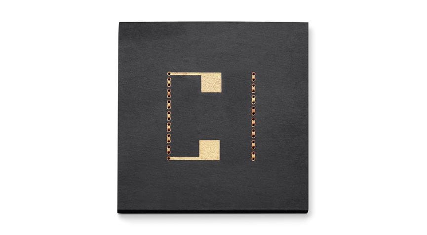 Magnetic fieldsensor, manufactured by means of injection moulding with laser directstructuring (LDS). The substrate used is the high-performance polymer TECACOMPPEEK LDS black 1047045 from Ensinger (Photo: Ensinger / IMPT).
Ensinger GmbH
Phone +49 7032 819 202
[obfemailstart]am9lcmcuZnJhbmtlQGVuc2luZ2VycGxhc3RpY3MuY29t[obfemailend]


