LPKF Laser & Electronics AG, a leading process in Molded Interconnect Device Technology - MID for short - conductor tracks can be generated on the surface of components. This makes it possible to integrate mechanical and electrical functions in a molded part in a unique way. With the LDS process, the conductive path is defined by a laser beam that writes the layout directly onto the injection-molded plastic part. For this purpose, a special LDS additive is added to the plastic during the manufacture of the compound. The desired component is first produced from this material, for example by means of plastic injection molding. Then the areas on which conductor structures are provided are processed with the laser beam and the added additive is then activated. During the subsequent metallization in an electroless copper bath, the conductive tracks on the activated surfaces are formed in an adhesive manner and with sharp contours. Different layers, for example nickel and gold, silver or solder, can be built up one after the other.
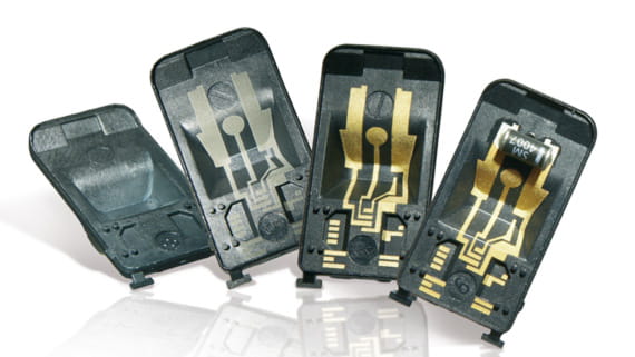
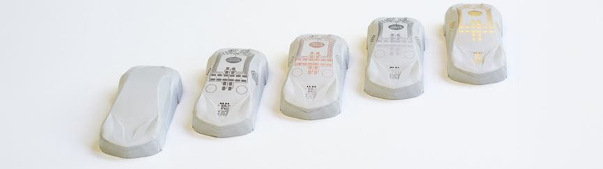
LDS is by far the most commonly used process for manufacturing MIDs. Mechatronic integrated components or molded interconnect devices (MID) manufactured with LDS can be used particularly well for functions such as:
Applications can also be found in medical, air conditioning and safety technology.
LDS requires the compound to have high heat resistance, good isotropic component behavior and, above all, good metallization properties due to the laser coupling behavior of the polymer and the ability to activate the additive. High temperature materials are required in particular for reflow soldering processes for passive components. In the LDS process, polymers are combined with metals. The difficulty here is that plastics generally have a much higher thermal expansion than metals. The TECACOMP LDS materials are optimised to this effect and have a very low thermal expansion.
In addition, TECACOMP PEEK LDS offer very good dielectric properties (TECACOMP PEEK LDS grey has a dielectric loss factor of 0,0006 with 1 GHz).
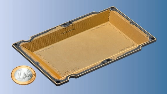
With the TECACOMP LDS materials, a surface roughness and an edge sharpness of the conductor tracks can be achieved, which enables a fine-pitch design up to 75 µm.
The TECACOMP LDS compounds are based on polyetheretherketone (PEEK) or liquid crystal polymer (LCP). By default, these compounds have a dark gray-black color, but with Ensinger's special filler concept, very light LDS structures can also be produced without copper-based additives, which can even be used in medical technology applications and are biocompatible in the case of PEEK LDS grey.
Ensinger is the only plastics processor in the world that can offer a PEEK for the LDS process that has been qualified by LPKF Laser & Electronics AG. The high-performance polymer is characterised by its high temperature resistance of up to 260 degrees Celsius (briefly up to 300 °C). It also has very good weld line strength, good adhesive strength and good chemical resistance. Through-hole plating (VIA) is possible. Important areas of application for the material TECACOMP PEEK LDS are antennas, sensors, heaters and security applications.
TECACOMP LCP LDS is particularly suitable for components with very thin walls. The liquid-crystalline material LCP is characterised by very good dimensional stability and rigidity. In addition, the plastic has good chemical and flame-retardant properties. Target industries are the consumer, electronics and automotive sectors.
Polymer |
Designation |
|
| PEEK | TECACOMP PEEK LDS | TECACOMP PEEK LDS black - 1047045 |
| TECACOMP PEEK LDS grey - 1061958 | ||
| TECACOMP PEEK MED LDS grey - 1067594 | ||
| LCP | TECACOMP LCP LDS | TECACOMP LCP LDS black - 1014978 |
The TECAFIL PEEK LDS black filament ist made of the Ensinger compound and is therefore adapted for the LDS process.
Ensinger offers the entire value chain from compounds to finished parts, injection molded or printed.
Ensinger has developed a concept that makes it possible to create sensors with very fine structures using thermoplastic material. The filler concept of TECACOMP PEEK LDS gray enables these structures with a surface roughness (Ra ~ 0.01 – 0.03 µm).
To date, applications below 40 µm have not been possible with LDS technology. In order to produce finer structures for microsystems technology, lithography processes are usually required and therefore substrates are used, which are usually based on silicon or ceramics. At this point, Ensinger offers the Ensinger Microsystems technology to enable finer structuring for microsystems in the plastic and the functionality vs. to increase compared to the conventional LDS. Various metallizations can be used for this in order to use the functional properties of different metals and alloys, for example to create thin-film-based sensors on polymer substrates such as TECACOMP PEEK LDS.